Package Competitiveness
Finding the technology of the package
In addition to the many technological implications of chip design, packaging technology has also made considerable progress. We can see that more and more IC products adopt higher threshold Bumping technology, multi-chip packaging and even SiP technology, as well as optical packaging and heterogeneous integrated packaging that are widely used in CIS products. Usually using these advanced packaged products, the package cost is even more expensive than the chip itself, and the yield problem will be more magnified due to further loss of the chip. Therefore, we believe that it is necessary to invest resources in the competitiveness analysis report for packaging to help our customers have better competitiveness
What can we bring for you?
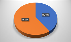
We will use SEM to measure the project, including the cross section of the substrate, the material analysis of the grid ball and the wire. In addition, we also have considerable experience in evaluating the cost of CP and FT testing. If you need to understand the routing of the substrate, we also have a wealth of experience to present the lines in each layer of the substrate.
With these analysis data, you can control cost more based on the development of products, and design more competitive products.
 |  |  |
|---|---|---|
 |  |  |
 |
