Uneven surfaces and 3D packaging
Uneven surface treatment or 3D packaging makes delayering the hardest part of the flow. Since mobile devices became ubiquitous, small-form, 3D and SiP multi-die packages have become common.

No amount of care in schematic recovery can make the result more accurate than the imagery it was built from. That is why decapsulation, delayering and imaging all happen in house.
Any one of them can be where a project stalls.
Grounded in experimental work on silicon and chemical reagents, samples are opened and decapsulated. A dedicated R&D team develops our own wet chemistry to suit different package materials.

RIE equipment performs reactive ion etching on the bare die, removing silicon dioxide, silicon nitride and similar dielectrics layer by layer. Depending on the part we also use CMP slurry with silicon carbide, or a chemical etch followed by polishing. Each method has trade-offs and both are often needed.

A modified scanning electron microscope with custom software captures imagery at large scale, wide area and very high speed, then our own stitching software assembles it into a complete die image. Magnification is chosen per layer according to process, composition and routing density.

Site-specific cross-sectioning, vertical structure SEM imaging and dimensional measurement. Resolving the structure of advanced processes helps customers judge process generation and layer construction accurately.

This is what delayering actually looks like — every layer has to be removed, refocused and imaged again, and no two look alike.
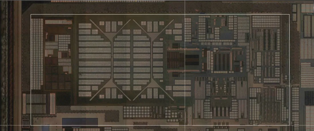
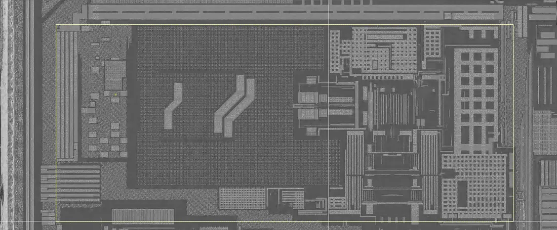
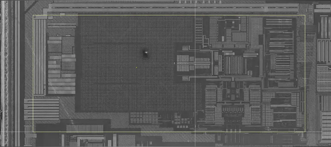
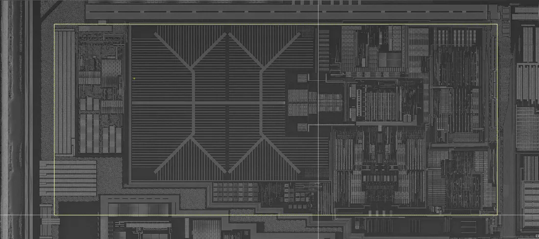
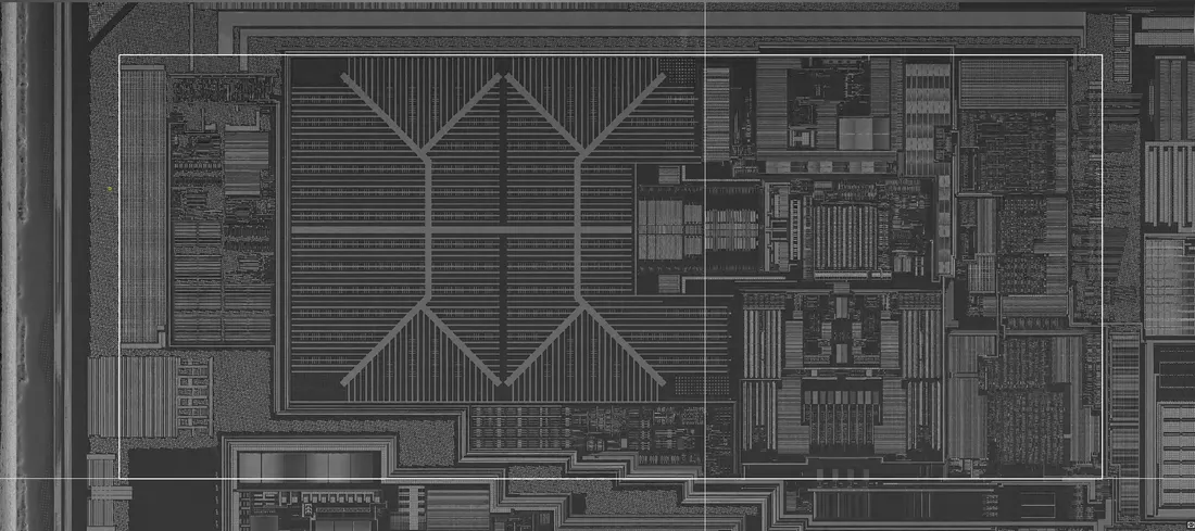
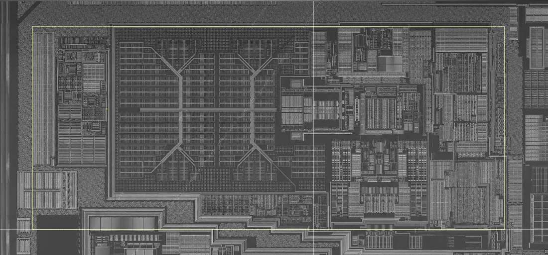
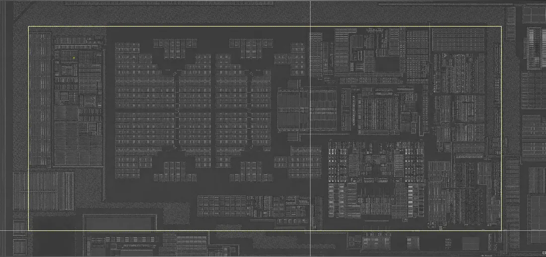
Below are seven layers of the same region on the same die. Stepping from M6 at the top down to the poly layer, the metal routing changes completely at each level until the devices underneath are exposed. Schematic recovery is the work of comparing these seven captures — and the layers below them — against one another.
Delayering is the most universal step in the lab, and the one most likely to stall.
Uneven surface treatment or 3D packaging makes delayering the hardest part of the flow. Since mobile devices became ubiquitous, small-form, 3D and SiP multi-die packages have become common.
The more layers, the harder cumulative delayering error is to contain — any one layer can be the one that writes off the whole part. We are currently working on 3D flash memory with more than 128 layers.
On the packaging side, we have successfully handled SiP assemblies containing as many as 10 ICs.
More than ten 3nm process ICs have now been analysed. In 2016, the node we had just solved was 16nm.
What the circuit analysis flow actually uses.
| Equipment | Used for |
|---|---|
| Scanning Electron Microscope SEM | Primary tool for layer-by-layer die imaging, and for observing cross-section structure |
| Focused Ion Beam FIB | Site-specific sectioning to prepare cross-sections for internal structure examination |
| Optical Microscope OM | Surface inspection and low-magnification imaging |
| Reactive Ion Etcher RIE | Removing silicon dioxide, silicon nitride and other dielectrics, layer by layer |
| CMP polishing CMP | Chemical mechanical polishing with silicon carbide, grinding metal and via layers at constant rate |
After separation, every layer needs its capture conditions decided again.
Once layers are separated, magnification is set per layer according to process, material composition and routing density. Different metal layers on the same die do not share the same conditions.
The large volume of captured frames is then stitched by our own software into a complete die image. That image is the sole basis for schematic recovery — and it is exactly what you step through layer by layer inside BrigenOne.

Advanced nodes, 3D packaging and SiP are all welcome for evaluation. The evaluation report tells you feasibility, scope and cost.
Get in touch